
GigaSens Camera HDK: put your algorithm inside the camera.
The Concurrent EDA Hardware Development Kit (HDK) opens the FPGA inside GigaSens high-speed CoaXPress and 10GigE Vision cameras to your own real-time image processing. Your core runs at the full sensor rate, in-line with the pixel stream, before a single byte reaches the wire.
Why build on the camera HDK
Your core slots into a fixed, hardware-validated datapath: no block-design editing, no IP packaging, no firmware code. Copy a working example, write one JSON manifest, build.
Native VHDL/Verilog at the full sensor stream, existing 8-bit streaming IP reused unmodified (the HDK measures your core's AXI-Stream width and inserts a width/rate adapter automatically), or C++ via Vitis HLS.
The manifest wires core parameters and status straight to GenICam: one write from your host software, live on the next clock. The GenICam XML, firmware bindings, and register-map docs are generated from the same manifest, so they can never drift.
Runtime bypass/compute selection is frame-boundary safe while streaming: A/B your algorithm against the raw image without stopping acquisition.
Only the HDK gives your logic direct access to the camera's two digital inputs and two outputs - drive triggers, strobes, or real-time flags straight from your core.
Six built-in hardware counters report frames, beats, and stall cycles at the compute socket, so throughput is measured on the camera, not guessed.
The FPGA datapath
Three high-speed cameras, one HDK
| GigaSens CV 1.1 CXP | GigaSens CV 2.0 CXP | GigaSens CV 2.0 10G | |
|---|---|---|---|
| Full resolution | 3,660 fps @ 1280 x 864 | 2,247 fps @ 1920 x 1080 | 536 fps @ 1920 x 1080 |
| Windowed | up to 86,600 fps @ 640 x 32 | up to 109,264 fps @ 1920 x 16 | higher rates at reduced ROI |
| Interface | CoaXPress CXP-12 x4 | CoaXPress CXP-12 x4 | 10GigE Vision |
| Sensor | Luxima LUX13HS, 10-bit | Luxima LUX19HS, 10-bit | Luxima LUX19HS, 10-bit |
| FPGA headroom | AMD Kintex UltraScale: ~1,600 DSP slices, ~300 block RAMs, ~150K LUTs free for your core | ||
| Memory | 2 GB DRAM | 2 GB DRAM | optional 8 GB DDR4 "memory camera" build |
| Datasheet (PDF) | CV 1.1 CXP HDK datasheet | CV 2.0 CXP HDK datasheet | CV 2.0 10G HDK datasheet |
Algorithm to camera in four steps
Simulation included: verify before you flash
A self-checking, image-in/image-out testbench runs your core through the full camera datapath in the free edition of AMD Vivado: feed in your own test images, compare the output against a bit-exact golden model, and exercise parameter writes and live bypass/compute switches - all before you ever touch hardware.
A bug caught in simulation costs you minutes at your desk; the same bug on the bench costs hours - a rebuild, a reflash, and lab time on camera hardware. Together with the built-in structural design audit, most cores go from first compile to a working camera in a single flash.

The testbench reads test images, runs them through your core, and writes the processed result out for comparison.
What customers build with it
 Binary imaging - 10x less data to the host
 Histogram equalization
 Real-time laser tracking with ROI
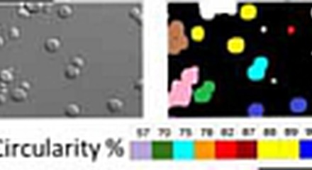 In-camera image classification
 Real-time 3D laser measuring
GigaSens cameras are built on Mikrotron® CoaXPress and 10GigE Vision platforms - more than 40 years of machine-vision pedigree, certified ISO 9001:2015 - with the FPGA opened up by Concurrent EDA for your own processing.